Atomic Structure Descriptor for Displacement Damage Defects in Semiconductors (AS4DS)
Content description of the project with basic funding information
The development of microelectronic devices that can work efficiently in a radiative environment (radiation hardening) represents a challenge for the present and future outer space exploration and exploitation [1]. In a highly radiative environment such as space or nuclear power plants, micro and optoelectronic components can be subject to Displacement Damage (DD) effects [2]. DD is a non-ionizing effect due to incident energetic particles (neutrons, protons, ions) in a radiative environment. It is described as a perturbation of the crystalline lattice by the displacement of atoms from their original positions, possibly creating point or defect clusters in the material. A similar effect can appear during ion implantation into wafers for example during manufacturing microelectronic process, where the incoming ion induces DD in the lattice of the target material. For more than thirty years, Molecular Dynamics (MD) simulations have proven themselves to be a very appropriate tool for the simulations of collision cascades in materials, and thus for the detailed understanding of DD [3, 4]. Collision cascades initiated by the Primary Knock-On Atom (PKA) have been extensively studied with MD giving a qualitative picture of the mechanisms at stake in materials. But the stochastic aspects of DD, the disorder it induced in the crystal [5] and the different times scales between the short time of the cascade and the long time of the annealing make it difficult to replicate numerically the evolution of damaged structures on realistic observable timescales compatible with available experimental data, and to meaningfully track and analyze the local atomic structure changes during the cascade evolution. Consequently, the fundamental understanding of the link between the changes at the atomic structure level and the resulting electrical effect measured on devices, remains a problem to be addressed.
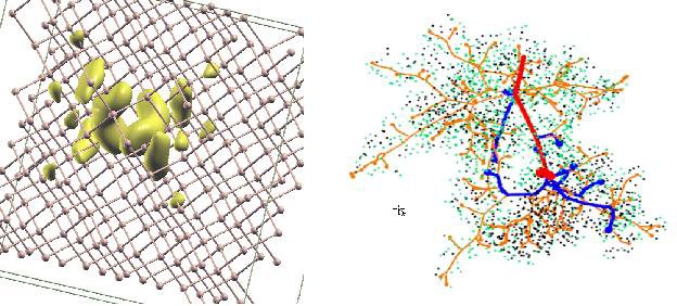
In the AS4DS project, we propose to develop a framework to describe and track structural changes occurring along cascade trajectories, the identification of defects and defect clusters in relevant materials, and keeping into account the statistical nature of cascades.
Funding: Project supported through the ARRS-CEA Bilateral Project “As4DS” NC-0018 (2021).
[1] https://assets.markallengroup.com//article-images/182082/P22-23.pdf
[2] J. R. Srour and J. W. Palko, IEEE Trans. Nucl. Sci. 60, 1740 (2013).
[3] M. Raine, A. Jay, N. Richard, V. Goiffon, S. Girard, M. Gaillardin, P. Paillet,
IEEE Trans. Nucl. Sci. 64, 133-140 (2016).
[4] A. Jay, M. Raine, N. Richard, N. Mousseau, V. Goiffon, A. Hemeryck, P. Magnan,
IEEE Trans. Nucl. Sci., 64, 141-148 (2016).
[5] P.D. Edmondson et al J. Appl. Phys. 106, 043505 (2009).
Composition of the project team
UNG:
• Matjaz Valant (Project leader; vodja) Bibliography
• Luigi Giacomazzi Bibliography
CEA:
• Nicolas Richard: Atomic Energy and Alternative Energies Commission (CEA), CEA-DAM-DIF
Project phases and their implementation
Workpackage 1 (coordinator: UNG)
• Task 1.1: Identification of descriptors and shape matching tools for tracing the local structure evolution during particle irradiation.
• Task 1.2: Further improvement of the protocol designed in Task 1.1. and automatization.
Current Status: in progress
Workpackage 2 (coordinator: CEA-DAM-DIF)
• Task 2.1: Testing of several candidate descriptors and shape matching tools on DD cascades test beds
•Task 2.2: Massive calculations of the local structure evolution, defect tracking and characterization of DD cascades in Si, Ge-Si and GaAs
Current Status: in progress
Bibliographic references
Publications: